
 Chinese
 English
 Russian
 French
 Spanish
 Arabic
 German
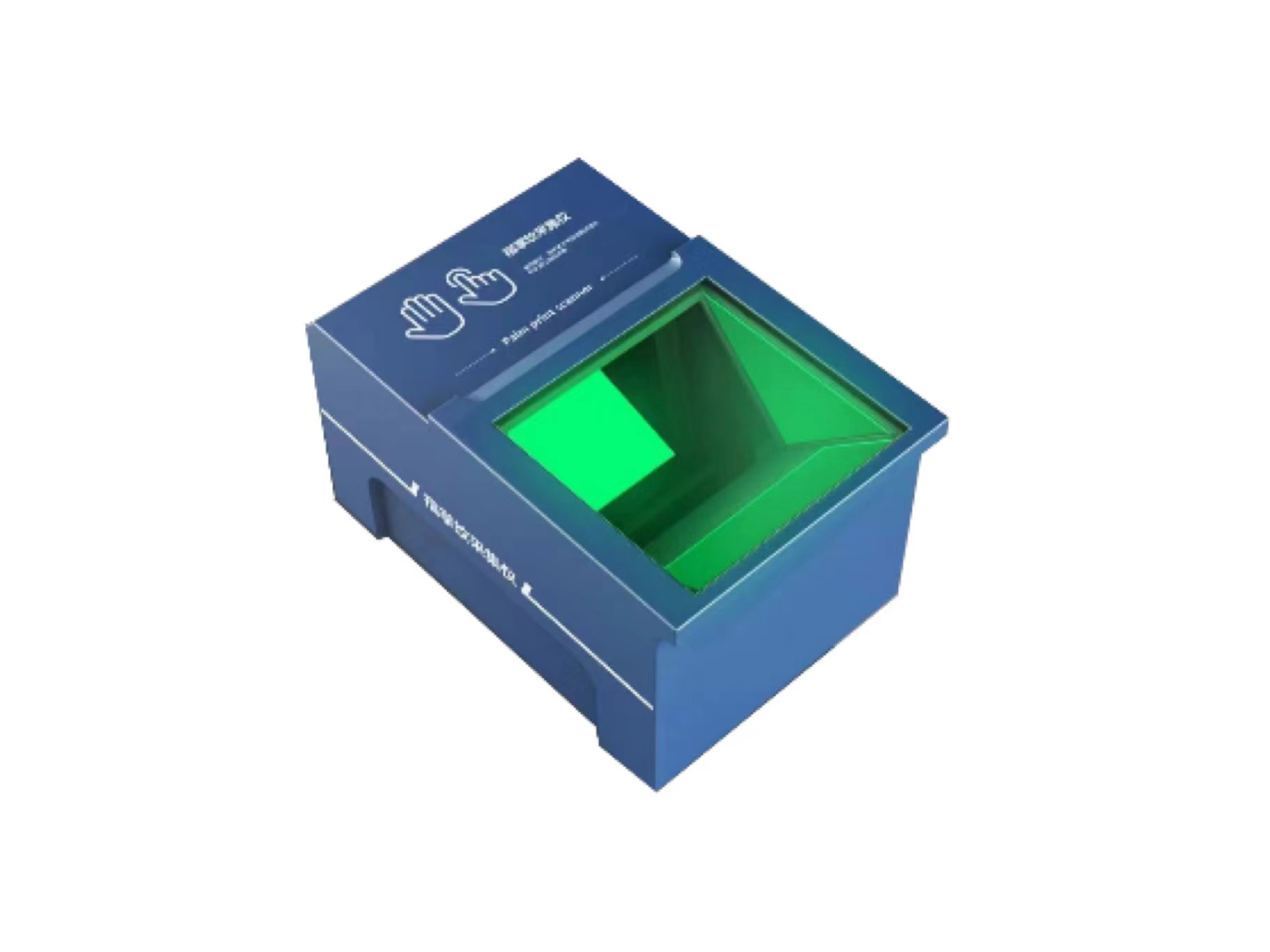
FBI FAP20 Fingerprint sensor
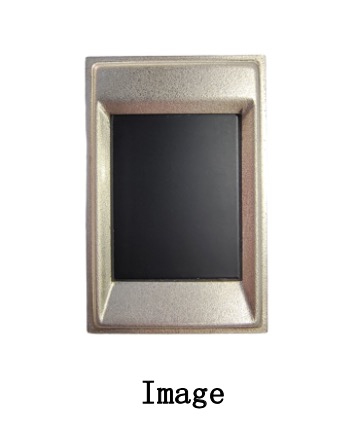
Describe:A9 is a high-performance fingerprint sensor developed independently by our company. This sensor has features such as full imaging surface area and low power consumption and meets the FBI FAP20 standard. It is a highly integrated capacitive sensor with high reliability, good adaptability to dry and wet fingers, and clear image acquisition. The sensor performs exceptionally well in terms of ease of use and durability. It is stable and has a long service life, and is well adapted to harsh conditions such as high and low temperatures and sandstorms. Combined with our company's fingerprint algorithm, it can normally collect fingers that are dry, cracked, dirty, wet, and so on, and has good comparison results.
Product features
High fingerprint quality: Capacitive fingerprint technology has a higher image quality.
High anti-counterfeit ability: Has strong ability to distinguish fake fingerprints.
Strong adaptability: Can normally collect fingers in dry, cracked, dirty, wet, and other conditions and has good adaptability.
International standards: Complies with the FBI FAP20 standard in the United States.
Interface description: Adopts high-speed QSQI communication interface and is compatible with SQI interface communication.
Features
1. 2D capacitive fingerprint area sensor
2. sensor array of 300x400 pixels
3. 508 DPI spatial resolution
4. 8-bit gray levels
5. 15.0 mm x 20.0 mm active sensing area
6. High speed SPI interface
7. Image capture speed up to 2 Mpixel/sec
8. ESD protection : + / - 15kV (Air mode)
9. Low power : Normal and Stand-by modes
10. > 3.5 million finger placements
11. FPC/FFC connection interface
12. SMD (SMT Device) design (optional)
Product technical parameters
Classification | parameter index | Parameter explanation |
Electrical parameters | Working voltage | DC-5V (Voltage range: 5V ± 10%) |
Working current. | 25mA | |
Static current. | 65uA | |
Sensor | Sensor Type | Semiconductor capacitance sensor |
Acquisition method | Planar pressing | |
Service Life | Greater than 1 million times (parameters provided by the manufacturer). | |
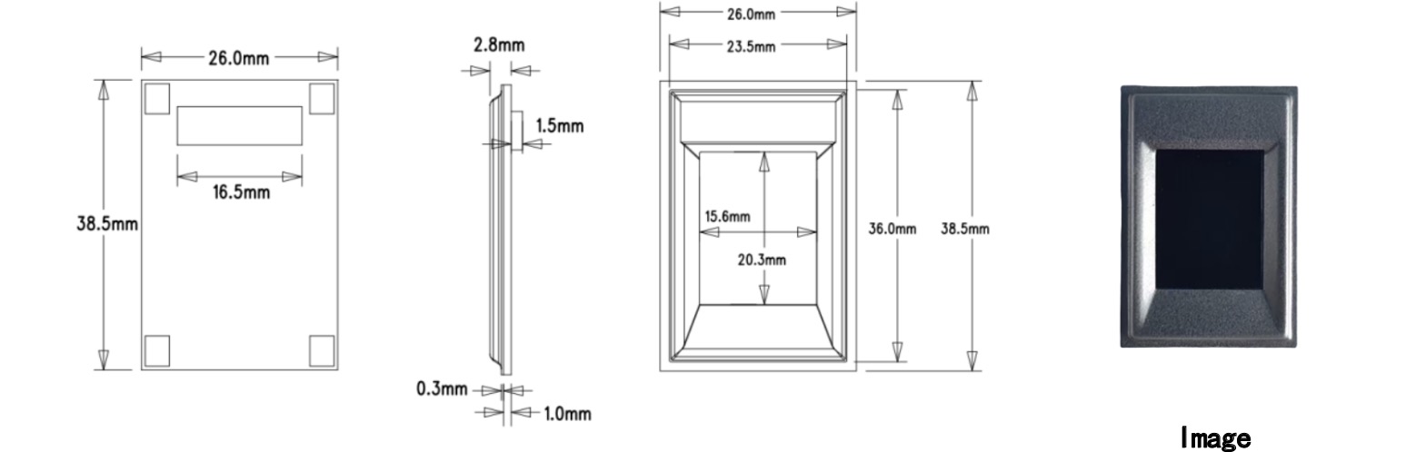
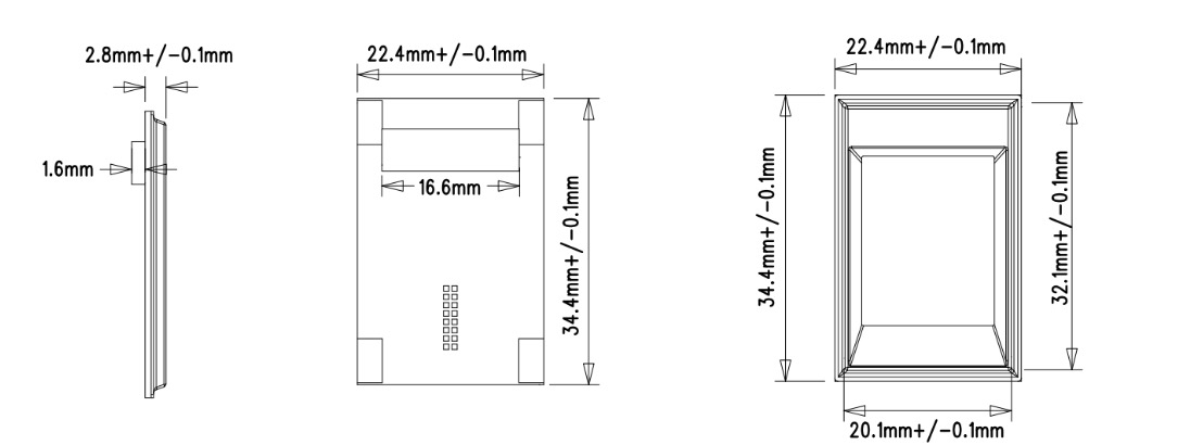
Module size(Two options are available) | 34.4x22.4x4.4mm(The frame size is compatible with FAP10) /38.5x26.0x2.8mm | |
Image pixels | 300*400pixel | |
Sensor size | 15.15 X 20.66mm | |
Image resolution | 500dpi | |
Gray level dynamic range | ≥150 | |
ESD(Air) | 15kv | |
ESD(Toutch) | 8kv | |
Cross cut | 5B | |
PencilHardness | 7H | |
RCA | >200 cycle | |
PIV | Certification | |
Working environment | Operating temperature | -20℃-+70℃ |
Storage temperature | -40℃-+80℃ | |
Working humidity | <90%R.H(Non-condensation) | |
Storage humidity | 20~93% R.H |
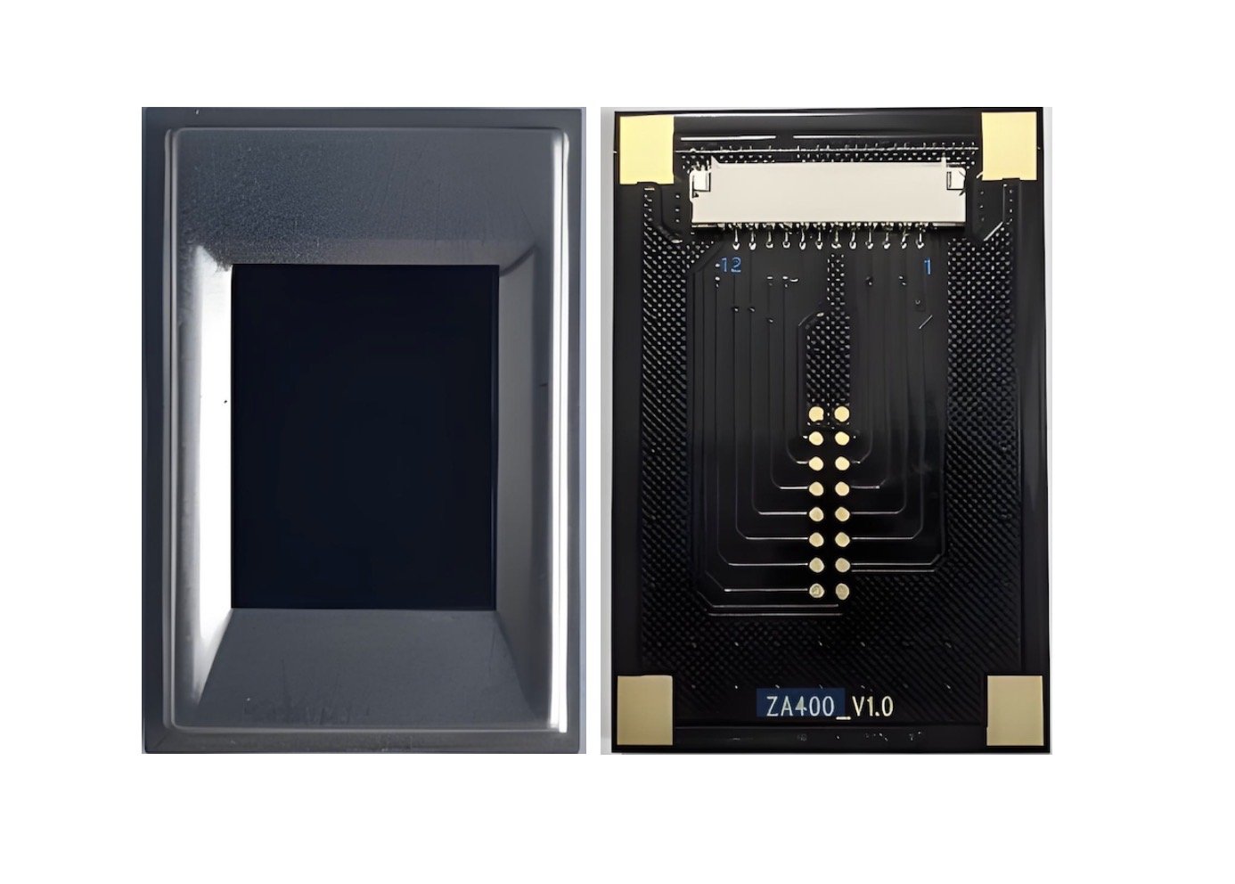
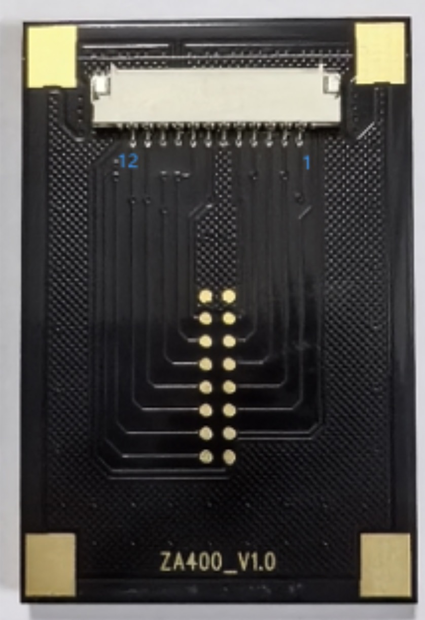
Interface definition
Pin number | PAD | Function description | Image |
1 | NC | NC |
|
2 | QSPI_MISO | SPI MISO | |
3 | VDD33 | 3.3V to 3.6V power input | |
4 | RESET | Module reset | |
5 | QSPI_SCK | QSPI CLOCK | |
6 | VSS | Ground | |
7 | QSPI_MOSI | Data I/O pins for QSPI interface. | |
8 | QSPI_CS | Chip select pin for SPI interface. | |
9 | ESD_GND | Ground the ESD pins. | |
10 | NC | NC | |
11 | QSPI_IO2 | Data output pins for QSPI interface | |
12 | QSPI_IO3 | Data output pins for QSPI interface |
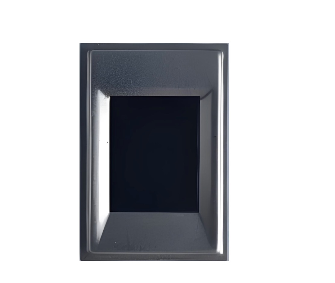
Product dimension drawing
- None
- None
Back To List


